Microscope image of electromigration-induced hillock and void
Por um escritor misterioso
Last updated 06 abril 2025
High magnification SEM micrograph of the notch area after

PDF) In-situ scanning electron microscope observation of electromigration-induced void growth in 30 nm ½ pitch Cu interconnect structures

Mitigation of Electromigration in Metal Interconnects via Hexagonal Boron Nitride as an Ångström‐Thin Passivation Layer - Jeong - 2021 - Advanced Electronic Materials - Wiley Online Library

In-Situ Observation and Quantitative Analysis of Electromigration Void Dynamics

Electromigration Reliability of Barrierless Ruthenium and Molybdenum for Sub-10 nm Interconnection

Mitigation of Electromigration in Metal Interconnects via Hexagonal Boron Nitride as an Ångström‐Thin Passivation Layer - Jeong - 2021 - Advanced Electronic Materials - Wiley Online Library
Micromachines, Free Full-Text

PDF) Hillock formation during electromigration in Cu and Al thin films: Three‐dimensional grain growth

Materials Quest for Advanced Interconnect Metallization in Integrated Circuits - Moon - 2023 - Advanced Science - Wiley Online Library

Microscope image of electromigration-induced hillock and void

Microscope image of electromigration-induced hillock and void
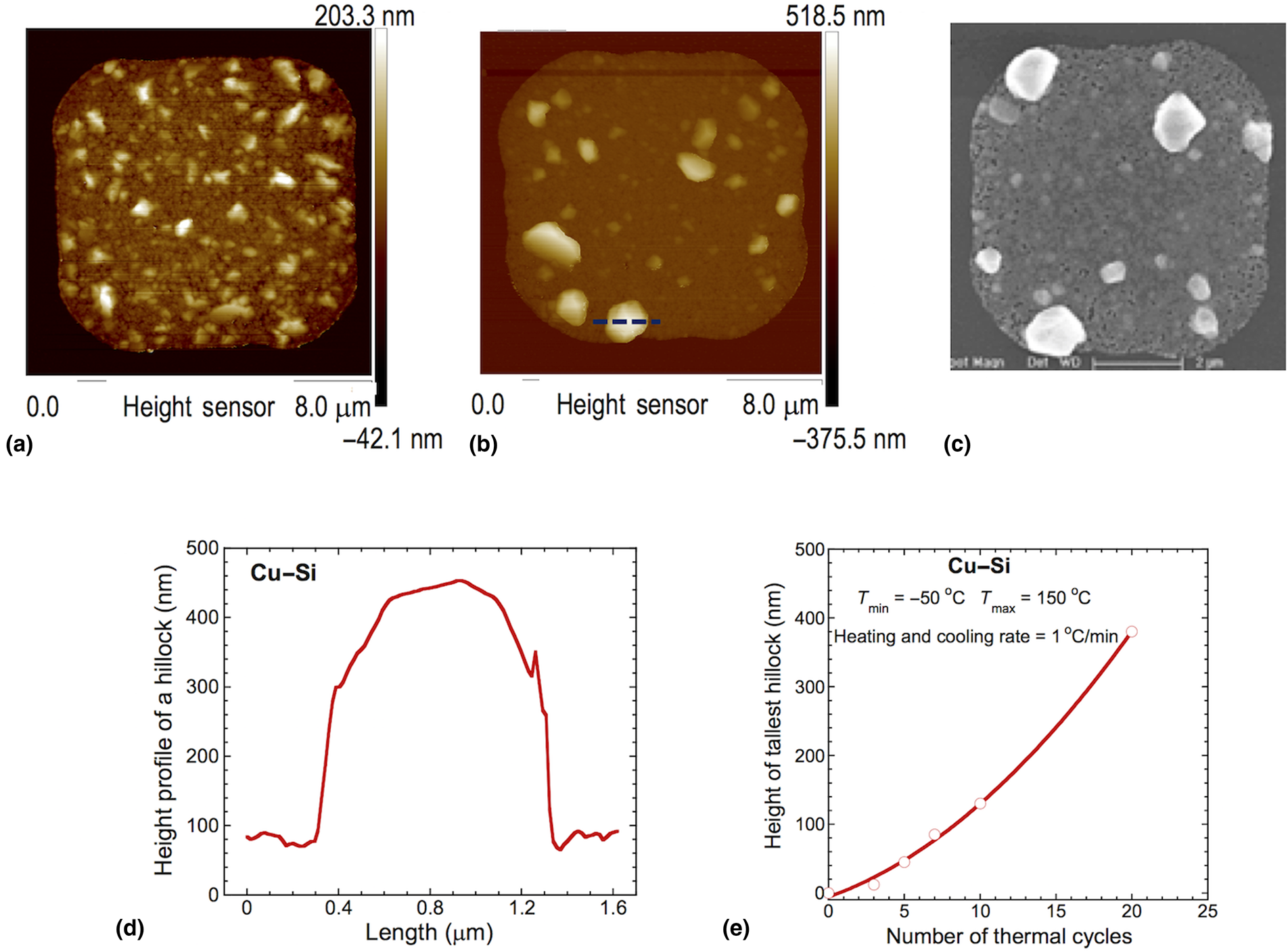
Effects of an interfacial layer on stress relaxation mechanisms active in the Cu–Si thin film system during thermal cycling, MRS Communications

PDF) Hillock formation during electromigration in Cu and Al thin films: Three‐dimensional grain growth
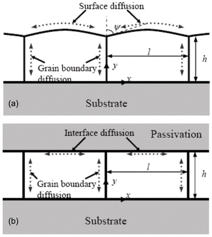
Thermal Stress Characteristics and Stress-Induced Void Formation in Aluminum and Copper Interconnects (Chapter 3) - Electromigration in Metals
Recomendado para você
-
 Hillock site hi-res stock photography and images - Alamy06 abril 2025
 -
 Hillock Hotels06 abril 2025
 -
 File:Hillock - panoramio.jpg - Wikimedia Commons06 abril 2025
 -
 Hillock Green at Lentor Estate © Official Page06 abril 2025
 -
 Hillock Wines - Klein Karoo Wines06 abril 2025
 -
 Developers of Hillock Green take a turn to shape their vision for06 abril 2025
 -
 Hillock Insurance Brand Identity Services06 abril 2025
 -
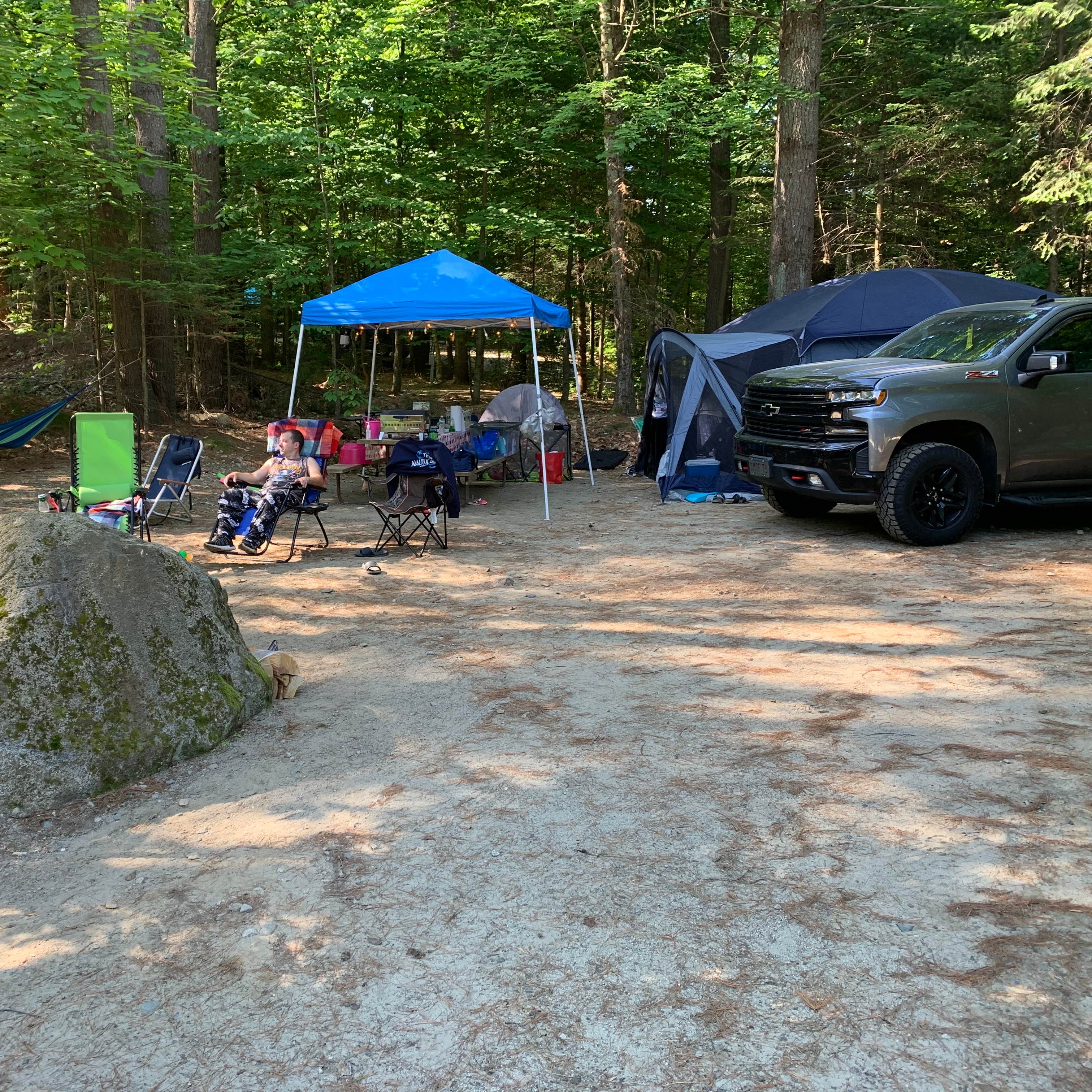 Moose Hillock Camping Resort Camping06 abril 2025
 -
 Hillock Green E Brochures06 abril 2025
 -
 Hillock Green at Lentor Central, New Condo06 abril 2025
você pode gostar
-
 Stranger Things Play': Cast, Release Date, Plot of The First06 abril 2025
 -
cabelo de menino de graça no roblox|Pesquisa do TikTok06 abril 2025
-
 10 jogadores do elenco do Flamengo já disputaram a Champions League06 abril 2025
 -
 De los pibes de Malvinas ¿que jamás olvidaré?06 abril 2025
 -
 Kimi no Na Wa - Your Name Vol. 1 - Edição Japonesa06 abril 2025
 -
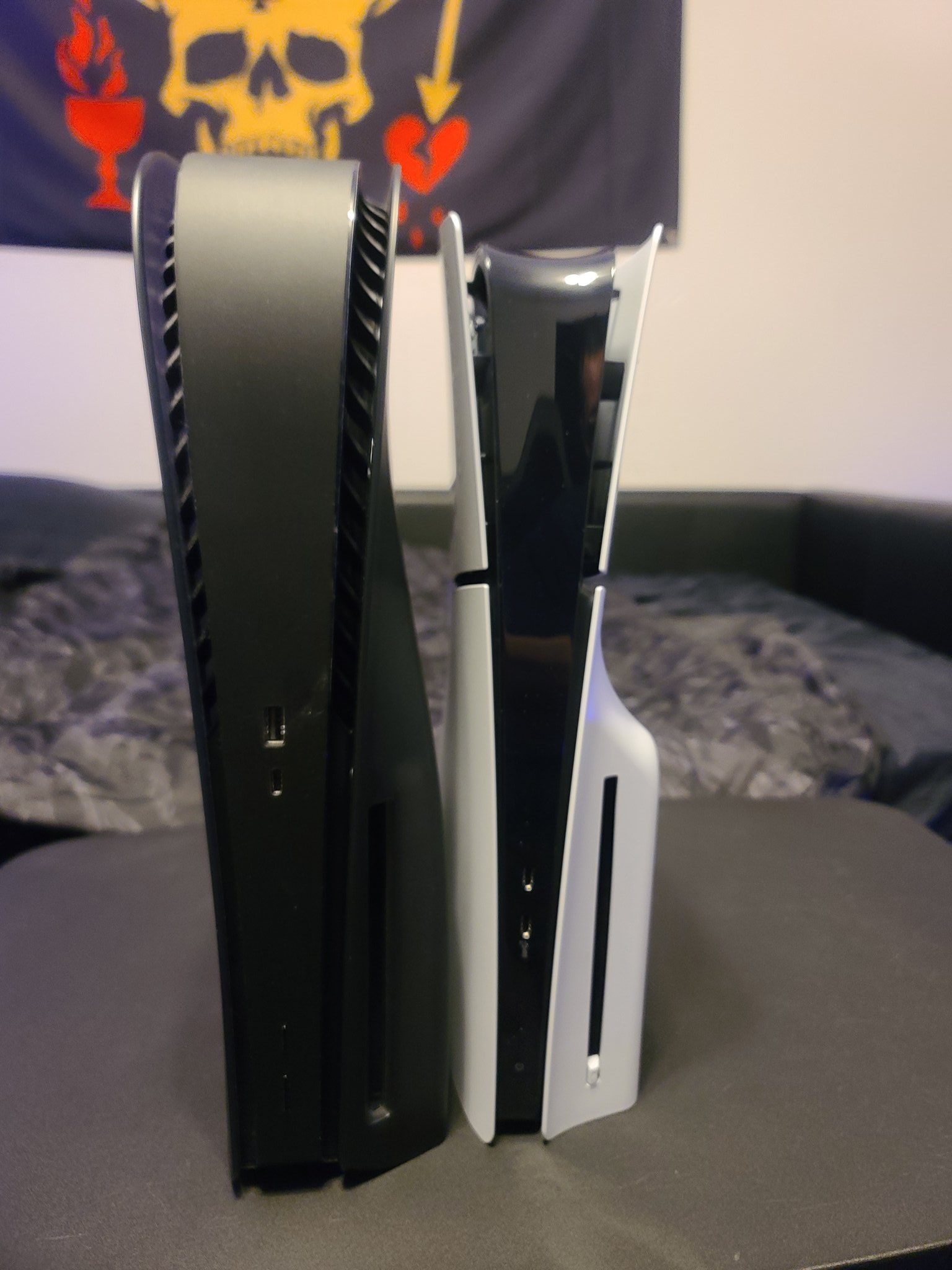 Slimmer PlayStation 5 already in some stores, disc drive requires online log in06 abril 2025
 -
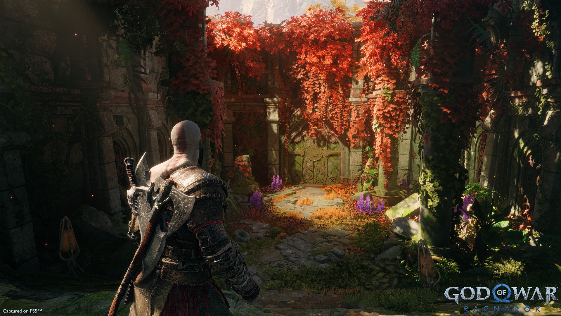 God of War Ragnarok Tech Analysis – A Visual Spectacle on PS5?06 abril 2025
 -
 gwen total drama island in my style|Pesquisa do TikTok06 abril 2025
 -
 Bigfoot Days festival returning to Estes Park in April 202206 abril 2025
 -
 Pokedex Gen 3 by Do0dledan06 abril 2025
